
Research Papers


Keep Reading
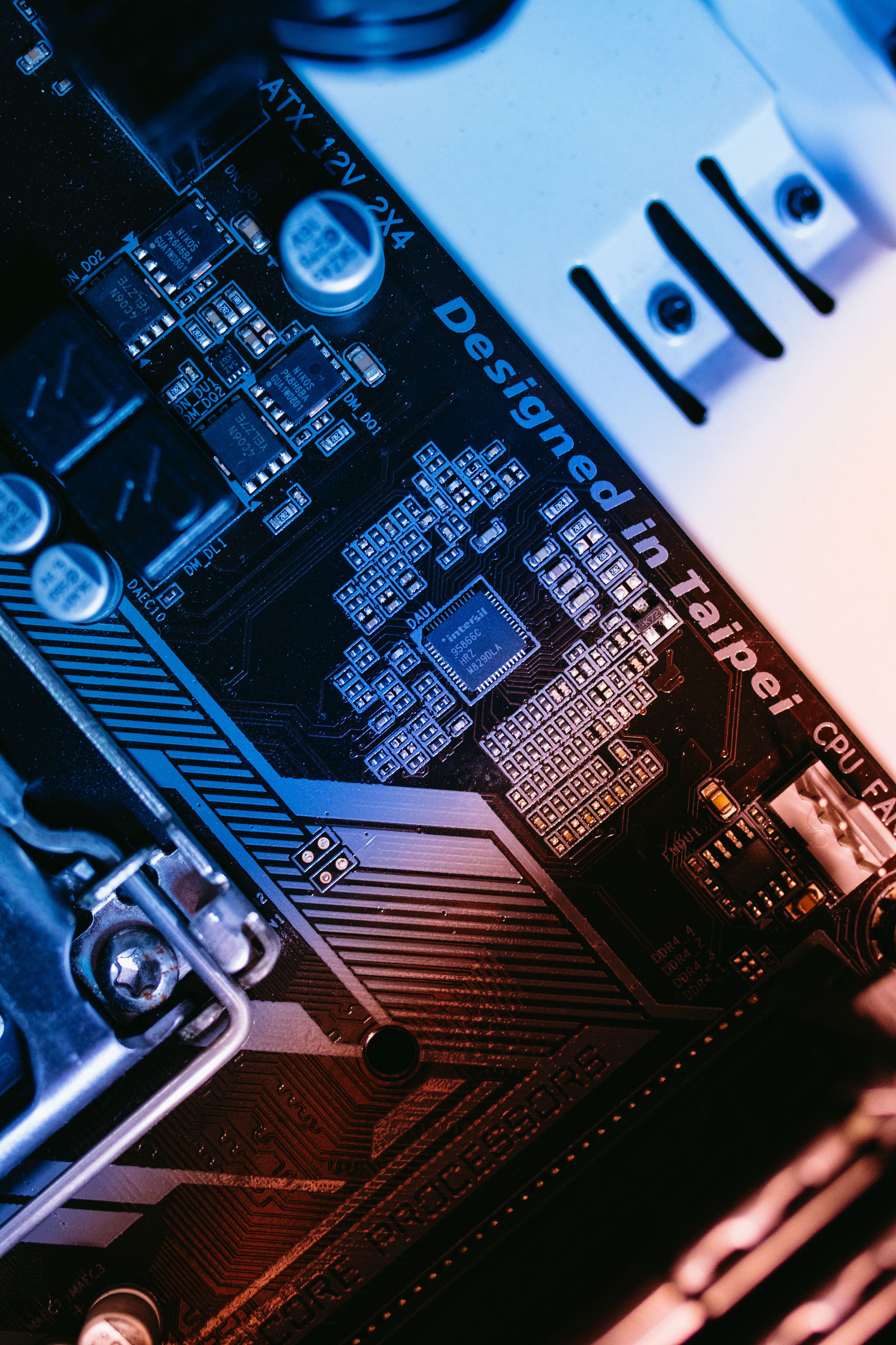
Wide-bandgap power semiconductors have become one of the most strategically important and most litigated areas in electronics, and their patent landscape is distinctive because value and risk are spread across the full stack from crystal to module. Silicon carbide and gallium nitride switch faster, tolerate higher voltages and temperatures, and lose less energy than conventional silicon, which is why they are central to electric-vehicle drivetrains, fast charging, solar and grid power conversion, and the power delivery of AI data centers; peer-reviewed reviews document these comparative properties and the trade-offs between the two materials.¹,² The intellectual property divides across several regions, each with different owners and maturity: the substrate and bulk-crystal growth that produces the raw material; the epitaxy that grows the active layers, including gallium nitride on silicon; the device design, such as the transistor and diode structures, whose failure and reliability modes are a distinct engineering concern;³ the packaging and thermal-management technologies that manage heat and switching losses;² and the application-level integration into drivetrains and power systems, where gallium-nitride high-electron-mobility transistors are increasingly used.⁴ Because a competitive product depends on several of these layers, freedom-to-operate is a multi-layer analysis rather than a single clearance.
The landscape is defined by intense litigation. Established wide-bandgap developers with deep substrate and device portfolios have asserted their patents against newer entrants, and the disputes have moved through trade-enforcement bodies and the federal courts. In a US International Trade Commission investigation into certain semiconductor devices, a final initial determination issued on December 2, 2025 found a violation as to one asserted patent and no violation as to a second, with the Commission determining to review the decision in part, a proceeding that remained under Commission review as of early 2026.⁶ In parallel, a wide-bandgap developer has asserted foundational gallium-nitride and silicon-carbide patents against a competitor in US federal court, with the case active on the district-court docket.⁷ Parallel proceedings are underway in other jurisdictions. This pattern signals a maturing field in which foundational substrate, epitaxy, and device patents create real barriers, and in which a single infringement finding in a key market can reshape a competitor's access to it. The ownership picture is concentrated but contested: across the Cypris corpus of more than 500 million patents and scientific papers, the most active assignees in the gallium-nitride power-device set are incumbent integrated device manufacturers, led by Japanese and European firms such as Mitsubishi Electric, Fuji Electric, Infineon, Toshiba, and Rohm, together with foundries and a small number of US developers, of which one substrate-and-device specialist is the clearest pure-play; the set holds on the order of 80,000 families on an indicative basis and grew roughly 2.4 times between 2018 and 2024, with China and the United States leading on assignee geography, followed by Japan, Germany, and South Korea. Because applications publish about eighteen months after filing, the most recent device and packaging filings are under-represented (2025 counts are partial), so the current frontier is more active than granted-patent counts suggest.
The strategic question is which layer to own, and the answer differs by material. In silicon carbide, the substrate and bulk-crystal layer is a durable barrier because high-quality crystal growth is difficult and capital-intensive, so much of the defensible value sits upstream. In gallium nitride, where devices are often grown on silicon wafers, the contested ground is more in epitaxy, device architecture, and packaging, and the litigation has concentrated there. Across both, packaging and thermal management are rising in importance as switching speeds increase,² and ultra-wide-bandgap approaches are an emerging frontier beyond today's materials.⁵ Reading the landscape by material, layer, and owner, and tracking the live proceedings, is what separates a workable position from a blocked one.
What creates FTO risk in wide-bandgap power semiconductors
Substrate and crystal-growth claims. These cover bulk silicon-carbide crystal and wafer production, a capital-intensive, upstream layer that is a durable barrier in silicon carbide.
Epitaxy claims. These cover the growth of active layers, including gallium nitride on silicon, a heavily contested layer central to gallium-nitride litigation.
Device-design claims. These cover transistor and diode structures and their edge terminations and gate designs, whose reliability and failure modes are a frequent center of disputes.³
Packaging and module claims. These cover thermal management, interconnection, and module construction, a layer rising in importance as switching speeds increase.²
Application-integration claims. These cover integration into drivetrains, chargers, and power systems, so a device can be free at the component level and constrained in a specific application.⁴
How AI-powered landscape and FTO analysis helps
A multi-layer, cross-border, heavily litigated landscape is beyond manual clearance. AI-powered analysis addresses this with semantic search that retrieves relevant substrate, epitaxy, device, and packaging claims regardless of terminology, attribution that normalizes incumbent and challenger owners to canonical entities across jurisdictions, claim-level analysis that separates the layers, and continuous monitoring that tracks new filings and the live disputes. Because wide-bandgap advances appear in scientific literature before they are patented, reading both patents and literature gives earlier warning of where the field is extending.
Where Cypris fits
Cypris runs patent landscape and freedom-to-operate analysis for multi-layer, litigated fields such as wide-bandgap power semiconductors across a corpus of more than 500 million patents and scientific papers, organized through a proprietary R&D ontology. The ontology clusters the landscape by material and layer, substrate, epitaxy, device, packaging, and application, and normalizes owners to canonical entities across jurisdictions, so a team sees how rights are distributed between incumbents and challengers rather than a flat list. Semantic search across patents and scientific literature surfaces relevant claims regardless of terminology and connects filings to the underlying materials and device research, which is where next-generation structures emerge first. Cypris Q, the platform's agentic layer, lets teams run landscape and FTO analysis conversationally and chain the attribution, clustering, and claim-level analysis across layers, and Agentic Monitoring tracks the landscape over time and flags new filings and developments as they publish. Cypris provides enterprise API partnerships with OpenAI, Anthropic, and Google, and is built with enterprise-grade security. Cypris serves hundreds of enterprise customers across pharmaceuticals, chemicals, advanced materials, energy, and other regulated industries.
FAQ
Why are wide-bandgap power semiconductors a patent hotspot? Wide-bandgap power semiconductors are a patent hotspot because silicon carbide and gallium nitride enable more efficient power electronics for electric vehicles, fast charging, renewables, and AI data centers, creating a large and fast-growing market. Value and risk are spread across substrate, epitaxy, device, and packaging layers. That breadth, plus intense competition, has produced heavy litigation.
What layers does the SiC and GaN landscape cover? The landscape covers substrate and bulk-crystal growth, epitaxy, device design, packaging and modules, and application integration. In silicon carbide the substrate layer is a durable upstream barrier, while in gallium nitride the contested ground is more in epitaxy, device design, and packaging. Freedom-to-operate must span the relevant layers for each material.
Why is this field so heavily litigated? The field is heavily litigated because foundational substrate, epitaxy, and device patents create real barriers, incumbents hold deep portfolios, and fast-growing challengers are building their own. Disputes have moved through the US International Trade Commission and the federal courts, with a December 2025 ITC determination finding a violation as to one patent and none as to another, and a separate district-court case over foundational gallium-nitride and silicon-carbide patents. A single ruling in a key market can reshape competitive access.
Where is the white space in wide-bandgap semiconductors? The white space includes packaging and thermal management as switching speeds rise, device architectures that design around crowded structures, gallium-nitride epitaxy and integration approaches, and application-level integration into drivetrains and power systems. The silicon-carbide substrate layer is a durable barrier held by incumbents. The higher-value opportunities are in packaging, device design, and integration.
How do silicon carbide and gallium nitride differ in the patent picture? They differ because silicon carbide value concentrates upstream, in difficult, capital-intensive crystal growth, while gallium nitride, often grown on silicon, concentrates contested IP in epitaxy, device architecture, and packaging. The litigation patterns reflect this. Freedom-to-operate strategy should therefore be tailored to the material.
Why does wide-bandgap analysis need scientific literature? Wide-bandgap analysis needs scientific literature because materials, device, and packaging advances appear in research before they are patented, so the literature gives the earliest signal. Analyzing patents alone gives a lagging view. Cypris analyzes both across more than 500 million patents and scientific papers.
What software helps analyze the SiC and GaN patent landscape? Software for the wide-bandgap landscape should cluster activity by material and layer, resolve incumbent and challenger owners to canonical entities across jurisdictions, search patents and scientific literature semantically, and monitor active litigation and new filings continuously. Cypris does this across more than 500 million patents and scientific papers using a proprietary R&D ontology, semantic search, Cypris Q, and Agentic Monitoring.
Which teams use wide-bandgap patent landscape analysis? Wide-bandgap patent landscape analysis is used by R&D, IP, and strategy teams at semiconductor, automotive, power-electronics, and energy companies, as well as investors assessing the sector. Because the field is litigated across the full stack and across borders, structured analysis is essential. Cypris serves hundreds of enterprise customers across advanced materials, energy, and other research-intensive industries.
Endnotes
- Stanley, C., Herzog, S., Viewegh, M., Biggerstaff, T., et al. (2026). Wide bandgap semiconductors for power electronics: comparative properties, applications, and reliability of GaN and SiC devices. Hardware, 4(1). https://doi.org/10.3390/hardware4010006
- Kim, J., Bae, S., Han, S., & Park, S. (2025). Thermal management of wide-bandgap power semiconductors: strategies and challenges in SiC and GaN power devices. Electronics, 14(21), 4193. https://doi.org/10.3390/electronics14214193
- Romano, G., Imburgia, A., Ala, G., Rizzo, G., et al. (2025). Comprehensive review of wide-bandgap devices: SiC MOSFET and its failure modes affecting reliability. Physchem, 5(1). https://doi.org/10.3390/physchem5010010
- Rusli, M., Jarndal, A., & Hamza, K. H. (2026). GaN HEMTs for electric vehicle power electronics: device architectures, reliability and next-generation wide-bandgap opportunities. Energies, 19(7), 1752. https://doi.org/10.3390/en19071752
- Adekunle, A. (2025). Review of ultra wide bandgap GaN-based HEMTs for high-efficiency power conversion. International Journal of Future Engineering Innovations, 2(3). https://doi.org/10.54660/ijfei.2025.2.3.77-83
- U.S. International Trade Commission. Certain semiconductor devices and products containing the same, Investigation No. 337-TA-1414 (Final Initial Determination, Dec. 2, 2025; Commission review in part). Federal Register / public-inspection record. https://public-inspection.federalregister.gov/2026-02297.pdf
- Wolfspeed, Inc. v. Navitas Semiconductor Corporation, U.S. District Court for the District of Delaware, No. 1:24-cv-01038 (docket). https://www.courtlistener.com/docket/69457003/parties/wolfspeed-inc-v-navitas-semiconductor-corporation
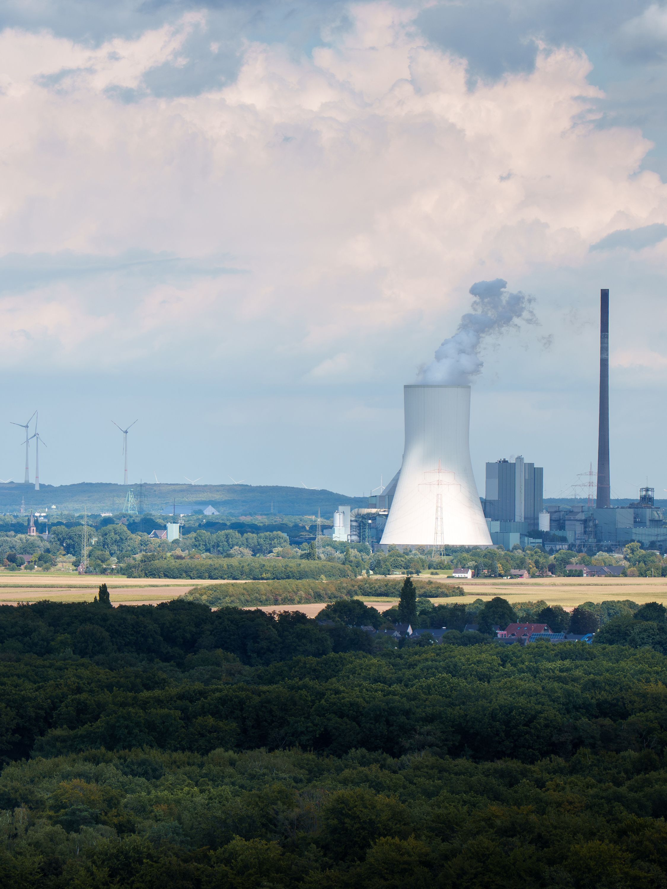
Small modular reactors and advanced nuclear designs have moved from concept toward licensing and deployment, and their patent landscape is distinctive because it spans several competing reactor families and a fuel supply chain that must be built alongside them. Where conventional nuclear plants are large, bespoke, and light-water-cooled, SMRs and advanced reactors are smaller, factory-built, and often use novel coolants, moderators, and fuels to achieve passive safety and flexible operation. The field divides into distinct regions of patenting: the reactor concepts themselves, including high-temperature gas-cooled reactors, molten-salt reactors, sodium-cooled fast reactors, integral light-water SMRs, and microreactors; the core, coolant, and moderator designs within each, from tristructural isotropic coated-particle fuel in gas-cooled reactors to fluoride fuel salts in molten-salt reactors;¹,²,³ the advanced fuels, especially TRISO particles and the high-assay low-enriched uranium, or HALEU, they require; the passive safety systems and control approaches that shut a reactor down without active intervention;⁵,⁶ and the modular manufacturing and construction methods that make factory production possible.⁴ Alongside these sit non-electric applications, from industrial heat and hydrogen to powering data centers. Because a viable design depends on several of these layers, and on a fuel supply that does not yet exist at scale, freedom-to-operate and white space analysis must span reactor, fuel, and manufacturing together.
The landscape is being reshaped by licensing progress and by a surge in demand. Regulators have modernized the framework for licensing advanced reactors, adopting a risk-informed, performance-based, and technology-inclusive rule intended to accommodate the range of SMR and advanced designs,⁷ while government programs are standing up a domestic supply of HALEU, the enriched fuel that many advanced reactors need and that has not been commercially produced at scale. Demand has accelerated sharply as technology companies contract for nuclear power to run data centers, drawing large investment. The competitive picture spans reactor developers pursuing different coolant and fuel choices, specialized fuel fabricators building TRISO and HALEU capacity, and established nuclear suppliers. This shows in the record: across the Cypris corpus of more than 500 million patents and scientific papers, the nuclear-anchored SMR, microreactor, TRISO, molten-salt, and HALEU set holds on the order of 2,017 families and grew from about 87 in 2020 to roughly 250 in 2024, with the most active assignees mixing large academic and institutional filers, led by Chinese universities and institutes, with reactor developers and fuel fabricators such as TerraPower, Mitsubishi Heavy Industries, BWXT, and Westinghouse and the US Department of Energy, and China ahead of the United States and South Korea on geography; a broad, unfiltered "microreactor" query returns far more families but is contaminated by unrelated chemical-microreactor art, so the nuclear-anchored figure is the defensible one. Because applications publish about eighteen months after filing, the most recent reactor and fuel filings are under-represented (2025 and 2026 counts are partial), so the current frontier is more active than granted-patent counts suggest.
The strategic question is which reactor family and layer to back, and the white space sits where technology and supply chain intersect. Advanced fuel, TRISO fabrication and the HALEU supply chain, is a critical, comparatively concentrated layer where scaling and cost are the barriers, so fabrication methods and fuel designs carry high value.¹ Coolant and materials that survive high temperatures and long fuel cycles, across gas, salt, and metal-cooled designs, passive safety systems, modular manufacturing and construction that lower cost and schedule, and non-electric applications such as process heat, hydrogen, and dispatchable power for data centers are all distinct, contested layers.²,³ Reading the landscape by reactor family, layer, and owner, and tracking both the patents and the underlying nuclear-engineering research, is what separates a crowded region from an open one.
Where the advanced-nuclear white space is
Advanced fuel and HALEU supply. TRISO fabrication methods and the high-assay low-enriched uranium supply chain are a critical, concentrated layer where scaling and cost are the barriers.¹
Coolant, moderator, and materials. Coolants and materials that survive high temperatures and long fuel cycles, across gas, salt, and metal-cooled designs, are a distinct, high-value layer.²,³
Passive safety systems. Systems and control approaches that shut a reactor down without active intervention are a differentiating capability central to SMR value.⁵,⁶
Modular manufacturing and construction. Factory-built modules and construction methods that lower cost and schedule are where the economic case is decided.⁴
Non-electric applications. Industrial heat, hydrogen production, and dispatchable power for data centers open distinct application and integration IP.
How AI-powered landscape and white space analysis helps
Resolving a landscape that spans several reactor families, a fuel supply chain, and manufacturing requires more than keyword search. AI-powered analysis addresses this with semantic search that clusters activity by reactor family, layer, and application across varied terminology, attribution that normalizes developer, fuel-fabricator, and supplier filers to canonical entities, and continuous monitoring that keeps pace with a fast-moving field. Because nuclear advances appear in scientific and engineering literature before they are patented, reading both patents and literature gives the earliest signal of where the frontier is moving.
Where Cypris fits
Cypris runs patent landscape and white space analysis for engineering-intensive fields such as small modular reactors and advanced nuclear across a corpus of more than 500 million patents and scientific papers, organized through a proprietary R&D ontology. The ontology clusters activity by reactor family, gas-cooled, molten-salt, sodium-cooled, light-water, and microreactor, and by layer, reactor design, advanced fuel, passive safety, and manufacturing, and normalizes developer, fuel-fabricator, and supplier filers to canonical entities, so a team can resolve which families and layers are crowded and which remain open as white space, and can separate genuine advanced-nuclear filings from unrelated art that shares terminology. Semantic search across patents and scientific literature connects filings to the underlying nuclear-engineering research, which is where advances appear first. Cypris Q, the platform's agentic layer, lets teams run landscape and white space analysis conversationally and chain the clustering, attribution, and gap analysis, and Agentic Monitoring tracks a defined family over time and flags new patents and papers as they publish. Cypris provides enterprise API partnerships with OpenAI, Anthropic, and Google, and is built with enterprise-grade security. Cypris serves hundreds of enterprise customers across pharmaceuticals, chemicals, advanced materials, energy, and other regulated industries.
FAQ
What is the small modular reactor patent landscape? The small modular reactor patent landscape is the set of patents covering factory-built, smaller nuclear reactors and advanced designs. It spans reactor families, high-temperature gas-cooled, molten-salt, sodium-cooled fast, light-water, and microreactors, plus advanced fuels, passive safety, and modular manufacturing. Each is a distinct region of patenting.
What are the main advanced reactor families? The main families are high-temperature gas-cooled reactors, molten-salt reactors, sodium-cooled fast reactors, integral light-water SMRs, and microreactors. They differ in coolant, moderator, fuel, and operating temperature. The choice of family shapes both the technical and the freedom-to-operate picture.
Why are TRISO and HALEU fuels important? TRISO and HALEU fuels are important because many advanced reactors depend on TRISO coated particles, which resist very high temperatures, and on high-assay low-enriched uranium, which is not yet commercially produced at scale. Building this fuel supply chain is a critical enabler. Fabrication methods and fuel designs are therefore a concentrated, high-value layer.
Why is data-center demand accelerating advanced nuclear? Data-center demand is accelerating advanced nuclear because technology companies need large amounts of reliable, carbon-free power, and have begun contracting for SMR and advanced-reactor output. This has drawn substantial investment and sharpened competition. It has also expanded interest in non-electric and dispatchable applications.
How does advanced-reactor licensing work? Advanced-reactor licensing in the United States distinguishes several steps, including design approval or certification, a construction permit, and an operating license, and regulators have adopted a modernized, risk-informed, technology-inclusive framework to accommodate advanced designs. A construction permit is not an operating license. Claims about a given project's status should be tied to the specific regulatory record.
Where is the white space in advanced nuclear? The white space includes advanced fuel and HALEU supply, coolant, moderator, and materials, passive safety systems, modular manufacturing and construction, and non-electric applications. The reactor-design and fuel layers are the most active. The most open, high-value opportunities are in fuel, materials, and manufacturing.
What software helps analyze the small modular reactor patent landscape? Software for the advanced-nuclear landscape should cluster activity by reactor family, layer, and application, resolve developer, fuel-fabricator, and supplier filers to canonical owners, separate genuine advanced-nuclear filings from unrelated art, search patents and scientific literature semantically, and monitor a fast-moving field continuously. Cypris does this across more than 500 million patents and scientific papers using a proprietary R&D ontology, semantic search, Cypris Q, and Agentic Monitoring.
Which teams use advanced-nuclear patent landscape analysis? Advanced-nuclear patent landscape analysis is used by R&D, IP, and strategy teams at reactor developers, fuel fabricators, nuclear suppliers, utilities, and technology buyers, as well as investors assessing the sector. Because the field spans reactor, fuel, and manufacturing layers, structured analysis is essential. Cypris serves hundreds of enterprise customers across energy and other research-intensive industries.
Endnotes
- International Atomic Energy Agency (2025). Coated particle fuels for high-temperature gas-cooled small modular reactors. https://doi.org/10.61092/iaea.zyya-k9sd
- Powers, J. J., & Gehin, J. C. (2016). Liquid-fuel molten salt reactors for thorium utilization. Nuclear Technology, 194(2). https://doi.org/10.13182/nt15-124
- Grimes, W. R. (1970). Molten-salt reactor chemistry. Nuclear Applications and Technology, 8(2). https://doi.org/10.13182/nt70-a28621
- Hannah, B. (2026). Technical assessment of molten salt reactor small modular reactors: design and licensing considerations. https://doi.org/10.5281/zenodo.20087242
- Zarei, M. (2020). State feedback control of power in a small modular reactor. Annals of Nuclear Energy, 144. https://doi.org/10.1016/j.anucene.2020.107743
- Diniz, R., et al. (2023). Reactivity calculation in molten salt reactors with an inverse kinetics model. Annals of Nuclear Energy, 190. https://doi.org/10.1016/j.anucene.2023.110130
- U.S. Nuclear Regulatory Commission (2026). 10 CFR Part 53 — risk-informed, technology-inclusive regulatory framework for advanced nuclear reactors (final rule). https://www.ecfr.gov/current/title-10/chapter-I/part-53
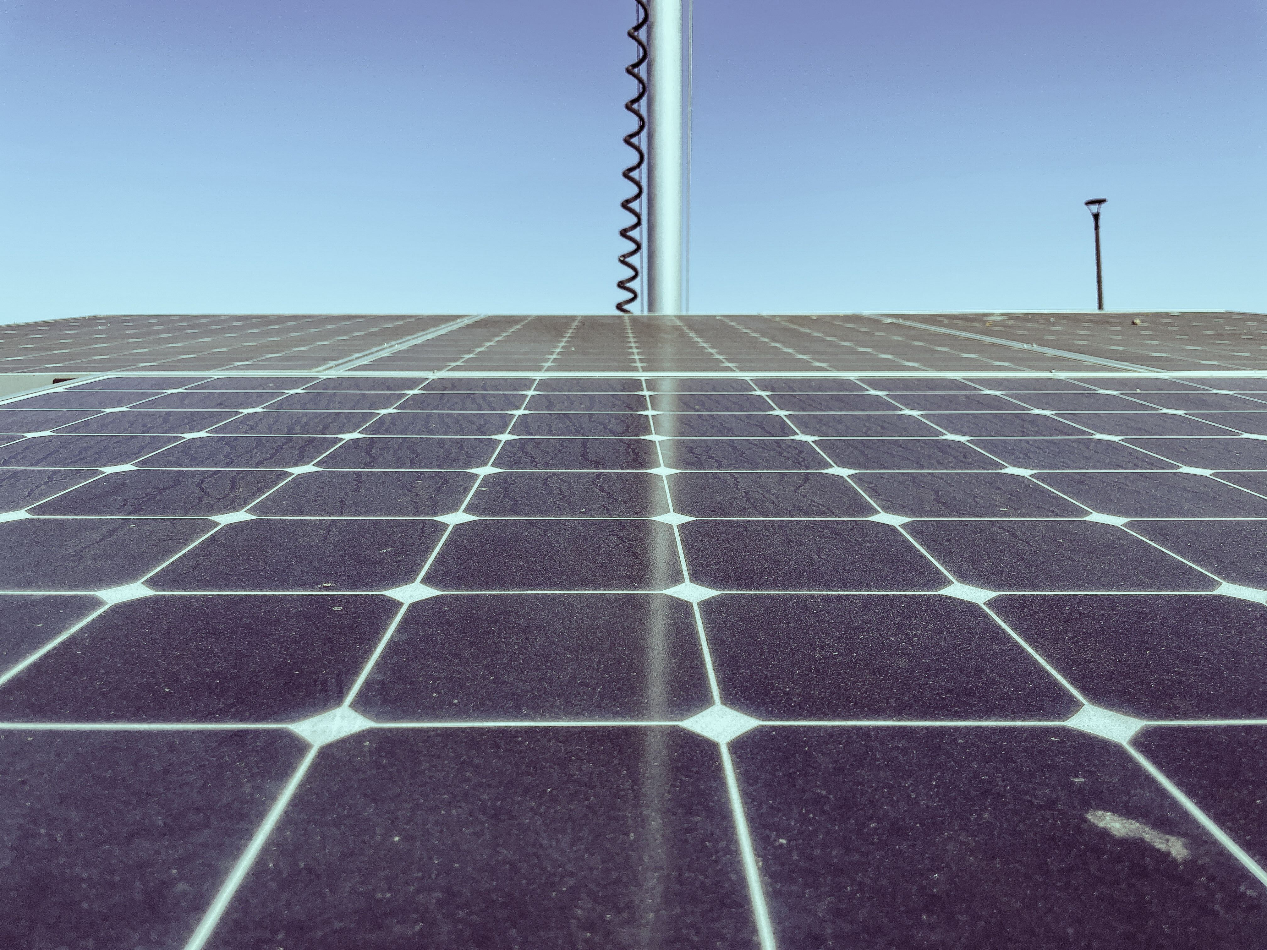
Perovskite-silicon tandem solar cells are the leading path to higher photovoltaic efficiency, and their patent landscape has become unusually central to competition because the field is commercializing through licensing as much as through manufacturing. A tandem cell places a wide-bandgap perovskite layer on top of a conventional silicon cell, so the two absorb different parts of the solar spectrum and the stack converts more sunlight than either alone, surpassing the single-junction limit that constrains standard silicon.¹,² The theoretical ceiling for a silicon-based tandem is about 43.2 percent, far above the roughly 33 percent limit of a single-junction silicon cell, which is what makes the architecture so attractive.³ The intellectual property divides across several regions, each with different owners and maturity: the perovskite compositions and their stability chemistry; the passivation and interface layers that raise efficiency and lifetime; the tandem device architecture, including the recombination layers that join the sub-cells; the texturing and deposition processes used to build the stack; and the encapsulation and manufacturing that make a durable module. Because a working tandem depends on all of these, freedom-to-operate and white space analysis must span the full stack.
The landscape is being shaped by patents and cross-licensing in real time. Certified efficiencies have climbed steeply: the current certified perovskite/silicon tandem record stands at 34.85 percent, achieved by LONGi and certified by the US National Renewable Energy Laboratory in 2025, and peer-reviewed work now describes certified perovskite/silicon efficiencies approaching 35 percent, with the live record register maintained on the NREL Best Research-Cell Efficiency Chart.⁴,⁵,⁶ These are laboratory cell records rather than commercial-module ratings, and translating them to industry-compatible cells and full modules is a distinct challenge the field is actively working through.¹⁰ Multi-junction routes are advancing in parallel, with triple-junction perovskite/perovskite/silicon devices exceeding 30 percent.⁷ Holders of strong foundational portfolios have begun licensing their technology to large manufacturers, signaling that IP position, not only manufacturing capacity, will determine who benefits from the transition. That structure is visible in the patent record: across the Cypris corpus of more than 500 million patents and scientific papers, the perovskite-tandem space is a comparatively small, fast-moving set of a few thousand de-duplicated families that stepped up sharply in 2025, and its most active assignees mix national laboratories such as CEA and CNRS, the perovskite specialist Oxford PV, and large silicon-module manufacturers, with China, the United States, South Korea, and France the leading jurisdictions; because assignee names are not fully canonicalized, manufacturer totals are best read as indicative. Because applications publish about eighteen months after filing, the most recent composition and process filings are under-represented, so the current frontier is more active than granted-patent counts suggest.
The strategic question is which layer to own, and the white space sits where durability is hardest to achieve. Perovskite stability under heat, humidity, and light remains the central unsolved problem, and the degradation mechanisms and stabilization techniques that address it are an area of intense, well-mapped research,⁸ as are the barrier and encapsulation designs that protect the cell over its service life.⁹ Compositions, passivation chemistries, and encapsulation that extend lifetime therefore carry high, defensible value, while tandem architecture and light-management texturing are contested and improving quickly, and scalable deposition and manufacturing are where laboratory records must survive the move to gigawatt production. Reading the landscape by composition, layer, and process, and tracking both the patents and the underlying materials research, is what separates a crowded region from an open one.
Where the perovskite tandem white space is
Stability and encapsulation. Compositions, passivation, and encapsulation that keep efficiency under heat, humidity, and light are the central unsolved problem and the highest-value, still-open target.⁸,⁹
Wide-bandgap perovskite compositions. Formulations tuned for the top cell that resist phase segregation are a contested, fast-moving composition layer.
Tandem architecture. Recombination layers, interconnection, and two-terminal versus four-terminal designs are a distinct device-engineering layer.⁷
Texturing and light management. Surface texturing and optical designs that maximize capture across the stack are an active process-IP area.
Scalable deposition and manufacturing. Moving high-efficiency processes from small cells to gigawatt-scale modules is where cost is decided and where durable process IP concentrates.¹⁰
How AI-powered landscape and white space analysis helps
Resolving a device landscape that spans compositions, interface and architecture layers, and manufacturing processes, across institutions and regions moving at different speeds, requires more than keyword search. AI-powered analysis addresses this with semantic search that clusters activity by layer and process across varied terminology, attribution that normalizes academic and commercial filers to canonical entities and tracks the licensing structure, and continuous monitoring that keeps pace with a fast-commercializing field. Because perovskite advances appear in scientific literature before they are patented, reading both patents and literature gives the earliest signal of where the frontier is moving.
Where Cypris fits
Cypris runs patent landscape and white space analysis for fast-commercializing energy fields such as perovskite tandem solar across a corpus of more than 500 million patents and scientific papers, organized through a proprietary R&D ontology. The ontology clusters activity by layer, perovskite composition, passivation and interfaces, tandem architecture, texturing and deposition, and encapsulation and manufacturing, and normalizes filers to canonical entities, so a team can resolve which layers are crowded and which remain open as white space, and can see the licensing structure clearly rather than as a flat list. Semantic search across patents and scientific literature connects filings to the underlying materials and device research, which is where perovskite advances appear first. Cypris Q, the platform's agentic layer, lets teams run landscape and white space analysis conversationally and chain the clustering, attribution, and gap analysis, and Agentic Monitoring tracks a defined layer over time and flags new patents and papers as they publish. Cypris provides enterprise API partnerships with OpenAI, Anthropic, and Google, and is built with enterprise-grade security. Cypris serves hundreds of enterprise customers across pharmaceuticals, chemicals, advanced materials, energy, and other regulated industries.
FAQ
What is the perovskite tandem solar patent landscape? The perovskite tandem solar patent landscape is the set of patents covering perovskite-silicon and all-perovskite tandem cells that exceed the single-junction efficiency limit. It divides across perovskite compositions and stability, passivation and interfaces, tandem architecture, texturing and deposition, and encapsulation and manufacturing. Each is a distinct region with different owners and maturity.
Why is IP so central to perovskite tandem solar? IP is central because the field is commercializing through licensing as much as through manufacturing, with holders of strong foundational portfolios licensing their technology to large manufacturers. Foundational process and architecture patents are concentrated among a few institutions and companies. That makes licensing and freedom-to-operate, not only production capacity, decisive.
What layers does the perovskite tandem landscape cover? The landscape covers perovskite composition and stability chemistry, passivation and interface layers, tandem device architecture including recombination layers, texturing and deposition processes, and encapsulation and manufacturing. A working tandem depends on all of them. Freedom-to-operate and white space analysis must span the full stack.
Where is the white space in perovskite tandem solar? The white space sits where durability is hardest: stability and encapsulation, wide-bandgap compositions that resist phase segregation, tandem architecture, light-management texturing, and scalable deposition. Stability under heat, humidity, and light is the central unsolved problem. The highest-value, most defensible positions are in lifetime and manufacturability.
Why is stability the key problem in the patent record? Stability is the key problem because perovskites can degrade under heat, humidity, and light, so the compositions, passivation, and encapsulation that extend lifetime are where the most valuable and defensible IP concentrates. Efficiency records matter, but durable modules require solving stability. The patent record reflects intense activity in these layers.
Why does perovskite analysis need scientific literature? Perovskite analysis needs scientific literature because new compositions, passivation chemistries, and device architectures appear in materials research before they are patented, so the literature gives the earliest signal. Analyzing patents alone gives a lagging view. Cypris analyzes both across more than 500 million patents and scientific papers.
What software helps analyze the perovskite tandem solar patent landscape? Software for the perovskite tandem landscape should cluster activity by device layer and process, resolve academic and commercial filers and the licensing structure to canonical owners, search patents and scientific literature semantically, and monitor a fast-commercializing field continuously. Cypris does this across more than 500 million patents and scientific papers using a proprietary R&D ontology, semantic search, Cypris Q, and Agentic Monitoring.
Which teams use perovskite tandem patent landscape analysis? Perovskite tandem patent landscape analysis is used by R&D, innovation, IP, and strategy teams at solar manufacturers, materials developers, and equipment makers, as well as investors and research institutions. It informs which layer to back, where to file, where to license, and where competitors are concentrated. Cypris serves hundreds of enterprise customers across energy, advanced materials, chemicals, and other regulated industries.
Endnotes
- Zhang, F., Shi, Y., & Berry, J. J. (2024). Perovskite/silicon tandem solar cells: insights and outlooks. ACS Energy Letters, 9(4). https://doi.org/10.1021/acsenergylett.4c00172
- Zheng, X., Tan, H., et al. (2023). Efficient perovskite/silicon tandem solar cells on industrially compatible textured silicon. Advanced Materials, 35(10). https://doi.org/10.1002/adma.202207883
- Schubert, M. C., Glunz, S. W., et al. (2025). Elucidating the efficiency limit of silicon-based monolithic tandem cells through the combination of Auger and Shockley-Queisser limits. EES Solar. https://doi.org/10.1039/d5el00085h
- Chen, W., Mularso, K. T., Jung, H. S., & Jo, B., et al. (2026). Strategies toward maximizing power conversion efficiency in all-perovskite tandem solar cells. Solar RRL. https://doi.org/10.1002/solr.202500911
- LONGi (2025, April 16). LONGi breaks world record for crystalline silicon-perovskite tandem solar cell efficiency (34.85%). https://www.longi.com/en/news/silicon-perovskite-tandem-solar-cells-new-world-efficiency
- National Renewable Energy Laboratory. Best research-cell efficiency chart. https://www.nrel.gov/pv/cell-efficiency
- Aydin, E., Xu, L., De Wolf, S., et al. (2024). Four-terminal perovskite/perovskite/silicon triple-junction tandem solar cells with over 30% power conversion efficiency. ACS Energy Letters, 9(8). https://doi.org/10.1021/acsenergylett.4c01292
- Ahn, N., & Choi, M. (2023). Towards long-term stable perovskite solar cells: degradation mechanisms and stabilization techniques. Advanced Science, 10(35). https://doi.org/10.1002/advs.202306110
- Yang, Z., Liu, Z., Chen, W., et al. (2020). Barrier designs in perovskite solar cells for long-term stability. Advanced Energy Materials, 10(26). https://doi.org/10.1002/aenm.202001610
- Jost, M., et al. (2021). 27.9% efficient monolithic perovskite/silicon tandem solar cells on industry-compatible bottom cells. Solar RRL, 5(6). https://doi.org/10.1002/solr.202100244